Elon Musk’s Terafab Targets 1 Million Wafers a Month by 2032
Credit: SpaceX
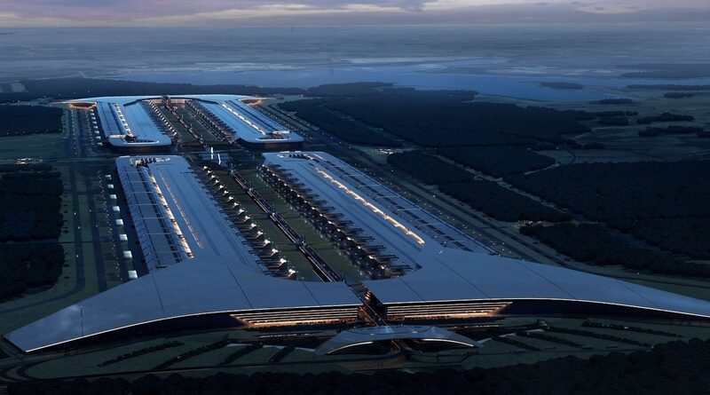
Elon Musk’s ambitious semiconductor venture, Terafab, is targeting a production capacity of up to one million silicon wafers per month after 2032, potentially placing the project among the world’s largest chip manufacturing operations.
According to recent industry reports citing Japan’s Nikkei, the planned facility will allocate approximately 700,000 wafers per month to memory production, while more than 300,000 will be dedicated to logic chips. The figures suggest that Terafab could eventually reach a memory manufacturing scale comparable to Samsung Electronics’ current DRAM production capacity.
Terafab plans an ambitious semiconductor expansion
Terafab is a joint semiconductor initiative involving Tesla and SpaceX, designed to secure a long-term supply of advanced chips for artificial intelligence, robotics and future computing infrastructure.
The project is being developed in Texas, with the broader objective of producing computing hardware capable of supporting up to one terawatt of annual computing capacity.
Unlike conventional semiconductor operations that rely on multiple specialized suppliers, Terafab aims to bring several stages of chip production under one roof. These include lithography, chip manufacturing, advanced packaging and testing.
This integrated approach could help Musk’s companies reduce their dependence on external semiconductor suppliers while gaining greater control over production schedules and hardware development.
Can Musk challenge Samsung’s DRAM dominance?
The proposed memory allocation is particularly significant. Samsung’s estimated monthly DRAM production capacity currently stands at approximately 650,000–700,000 wafers.
If Terafab achieves its stated target of 700,000 memory wafers per month, its planned capacity would be comparable to Samsung’s current DRAM manufacturing scale.
However, an important distinction remains: Terafab’s announced allocation covers memory chips in general, and the company has not publicly confirmed that all 700,000 wafers will be used exclusively for DRAM production.
Nevertheless, the scale of the ambition highlights Musk’s growing interest in controlling the semiconductor technologies needed for AI systems, autonomous vehicles and humanoid robots.
Production timeline remains a major challenge
Terafab is reportedly targeting the start of mass production in the second half of 2028, with its much larger capacity ambitions extending beyond 2032.
The project has already begun engaging semiconductor equipment suppliers in Japan, according to recent industry reporting. However, securing the necessary manufacturing equipment and meeting the proposed delivery schedules could prove difficult.
Building an advanced semiconductor fabrication facility requires substantial investment, highly specialized equipment and years of technical development. Even established manufacturers face considerable challenges when expanding production at this scale.
Intel is also expected to play a role in Terafab’s development, although the precise structure of its technical involvement has not been fully disclosed.
A potential new force in the global chip industry
If successful, Terafab could become a strategically important part of the semiconductor supply chain, giving Tesla and SpaceX greater control over the chips powering their future technologies.
For now, the one-million-wafer target remains a long-term ambition rather than an established production capability. Much will depend on investment, equipment availability and whether the companies can translate their aggressive timetable into reliable manufacturing operations.