NEO Semiconductor Demonstrates 3D X-DRAM Concept
Credit: NEO Semiconductor
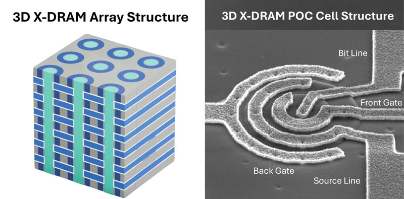
NEO Semiconductor, a developer of high-performance memory solutions, has demonstrated a proof-of-concept design for 3D X-DRAM, a multilayer DRAM technology designed to dramatically increase storage density and performance.
A key moment in NEO Semiconductor’s development was the acquisition of Stan Shih, an investor legendary in the electronics world. He is 81 years old and the founder of Acer, having led TSMC for nearly 20 years. Also significant was its collaboration with Taiwanese universities—National Yangming Chiao Tung University (NYCU) and its subsidiary, the Industry-Academia Innovation School (IAIS). The prototype was also manufactured in Taiwan, at the National Institutes of Applied Research—Taiwan Semiconductor Research Institute (NIAR-TSRI).
Testing and characterization of the sample were likely also conducted at NIAR-TSRI. The company reports read/write latency of less than 10 ns, refresh time at 85°C of over 1 second (15 times better than the JEDEC standard of 64 ms), and wearout tolerance of up to 10¹⁴. Noise immunity was also high.
“I am pleased that, thanks to the close partnership between industry and academia, we were able to validate the feasibility of NEO’s 3D DRAM concept in real-world silicon manufacturing conditions,” said Jack Sun, senior vice president of NYU and dean of the Institute for Applied Research in Science and Technology, and former CTO of TSMC. “This successful proof of concept not only demonstrates the potential of innovative memory architectures but also validates the feasibility of implementing advanced memory technologies using proven processes.”
NEO Semiconductor is actively promoting this technology, positioning it as a future replacement for traditional DRAM, especially for high-capacity and high-speed applications such as artificial intelligence.


